A new technique for scalable production of twisted van der Waals heterostructures has been used to produce twisted stacks with far more layers than previously possible. The applications are as yet unclear, but it could allow engineers to make use of the many fascinating phenomena discovered in twisted multilayer heterostructures such as superconductivity.
Following theoretical predictions by Allan MacDonald of the University of Texas at Austin and colleagues, Pablo Jarillo-Herrero at the Massachusetts Institute of Technology and colleagues showed in 2018 that in bilayer graphene, if the sheets were twisted relative to each other by just 1.1°, the material could become either a superconductor or an insulator. Subsequently, Jarillo-Herrero’s group and others have discovered exotic behaviour in graphene comprising three, four and five layers, as well as in twisted multilayers of materials like transition metal dichalcogenides and heterostructures.
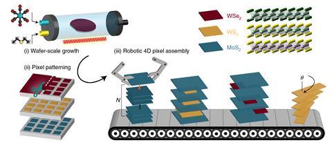
Producing these structures, however, involves carefully searching for monocrystalline regions on the surface of the bulk material, mechanically exfoliating them and finally stacking them at the required offset angle. Andrew Mannix, Jiwoong Park and colleagues at the University of Chicago in Illinois and elsewhere wanted a more scalable method. Wafer-scale versions of 2D materials ‘good enough for LEDs and transistors’ can now be produced using chemical vapour deposition, Park explains. ‘We were asking how to integrate these large-scale materials into devices in which these complicated structures can be produced in large quantity and with high throughput,’ he says.
The technique involves a wafer of each material being automatically cut into a large number of identical, pre-programmed and customisable shapes. A robotic arm is then used to pick up the monolayer, move it to the next wafer, twist it by the desired angle and stack it on top. In this way, an entire heterostructure can be assembled in a process similar to silicon chip manufacturing today. The wafers are of uniform quality, so each wafer can be cut in the same position, allowing parallel processing of the manufacturing process with no need to seek out perfect single crystalline regions and carefully position them over one another. ‘All the basic pieces have been there,’ Park explains. ‘Just like everything else what’s really important is the will to integrate everything.’ When the researchers tried the technique with exfoliated samples, the quality of the material was preserved – so the quality of the finished heterostructure is limited only by the quality of the wafers.
The researchers produced and characterised several heterostructures that could not be fabricated using current methods, such as one comprising 25 layers of molybdenum disulfide diagonally interspersed with tungsten disulfide. ‘We did clear optical spectroscopy measurements on all these materials continuously as we were adding one layer, then another layer, and what we found – which was somewhat surprising – was that the individual colours just add up like paint, and it becomes denser and more opaque. That’s something you would expect if it were a completely non-interacting material.’
The heterostructures eschew graphene and hexagonal boron nitride because reliably separating these from their growth substrates and depositing them in heterostructures without damage is not, at present, practical, says Park. The researchers can produce heterostructures at a speed of around 30 layers per hour, and Park believes this could be improved significantly with commercial investment. ‘The question is always what is it going to replace and for what reason?’ Park says. ‘We show that this is possible and hopefully it will allow people to think more freely.’
David Goldhaber-Gordon of Stanford University in California, who was not involved in the research, is impressed. ‘When I imagine trying to make a four- or five-layer twisted graphene stack with basically manual techniques, I find it terrifying,’ he says. ‘When I talk with people in the field, they often say, “We make 20 samples and we take the one that works well”. You can do a lot of good that way. but I think this method that Andy and Jiwoong have demonstrated really offers confidence about being able to make multiple samples with the same structure accurately and also opens up a realm of tens of layers that just wouldn’t happen with manual techniques.’