Controlling the chirality of organic semiconductors could enhance their efficiency and bring new functionalities to devices. However, manufacturing materials with tuneable chirality in bulk has remained a challenge – so far only a few examples of oriented monolayers had been reported. Now, a multidisciplinary team of researchers in the UK, Canada and Japan has developed a simple templating method to grow ordered chiral thin films for a wide range of applications.
‘Thanks to computational design and clever synthesis we knew we had really exciting materials,’ says lead author Jess Wade from Imperial College London, UK. ‘Organic semiconductors already showcase interesting properties, they’re lightweight, low-cost, biocompatible and highly tuneable.’ Adding chirality to the list could enhance the existing properties of optoelectronics, used in displays, sensors, solar panels, transistors and more. ‘Moreover, with chirality, we can manipulate the spin of photons and electrons at room temperature,’ she says. ‘But to do that in devices, we needed to control chiral properties in the bulk.’
To achieve this unprecedented control of chiral properties, researchers used a vacuum-based deposition technique, which works in combination with both organic and inorganic templates. ‘With his approach, [we] grow ordered thin films of helicenes on top of templating layers,’ explains Wade. Unlike previous approaches, which gave mostly monolayers only a few atoms thick, this new solution produces organised films 20 times thicker – up to 200nm. ‘The limit is the amount of molecules our amazing chemists can synthesise!’ she adds. This technology is much more precise in terms of closely controlling and monitoring the process.
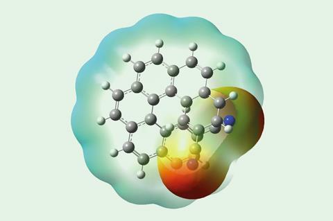
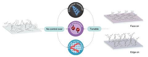
The deposition is quite simple – researchers take the chiral helicenes in powder form, heat it up, and let it sublimate onto the templates. ‘These particular helicenes arrange in supramolecular columns, and we found [they either] lie flat or stand upright, which has a huge impact on their optical and electronic properties,’ adds Wade. ‘Depending on our choice of templating layer, the helicenes orient in different directions.’
On the one hand, a template based on a polyaromatic organic molecule leads to the formation of helicene columns that align perpendicular to the surface. On the other, an inorganic template, like copper iodide, favours the formation of flat-lying columns – possibly because of interactions between helicenes and the negative charge at the surface. They each have distinct properties, including light absorption and x-ray diffraction.
‘Helicenes [are] known to display very strong chiroptical activity,’ explains Jeanne Crassous, an expert in chiral materials at the Rennes Institute of Chemical Sciences in France. ‘This result is important because [it] controls the orientation of semiconducting materials … in a very simple manner,’ she adds. Crassous also highlighted the key role of collaboration in this work. ‘[The team] gathers a unique association of synthetic chemists, theoreticians and physicists, which allows them to make simple and original ideas concrete.’
Ghislaine Vantomme, who explores chiral materials at Eindhoven University of Technology in the Netherlands, agrees. The discovery happened because ‘people from very different backgrounds talked together and worked together’. Furthermore, Vantomme notes the importance of computational studies. ‘The templates start crystallisation, but identifying the right match between the templating layer and the small chiral molecule requires hard work and a lot of computation.’ The calculations helped simulate the crystal structure of the helicene columns, which also contributed to the complete characterisation of the self-assembled structures. ‘Controlling the alignment of molecules is very difficult, but really important to the functionality of the devices,’ she adds.
Both Crassous and Vantomme agree this study is a stepping stone towards many more chiral materials, devices, and applications. ‘At the moment, they tried a few different helicenes and templates,’ explains Vantomme. ‘The types of structures [and] interactions open the door to new possibilities,’ she adds.
The main drawback, explains Wade, is the availability of enantiopure helicene. ‘Sometimes the most incredible molecules are complicated to synthesise,’ she says. In this case, ‘it’s even harder to separate them into enantiomerically pure forms’. But, when that’s solved, ‘this method may indeed become scalable and cheap, thus promising for applied developments in devices’, explains Crassous. ‘The applications are numerous and promising, from lighting to energy production,’ she adds.
Like liquid crystal technology, which started small and ended up in all our screens, this technology has huge potential, comments Vantomme. ‘For example, chiral materials could improve the efficiency of OLEDs, a market that’s worth billions,’ she adds.