The transistor has ceased its shrinkage. Not merely decelerating or backing off, but actually encountering a barrier dictated by atomic size and quantum mechanics principles. For approximately sixty years, the entire premise of computing was built on reducing these diminutive switches and fitting more of them onto a flat silicon sheet. This approach was exceedingly effective. It was so successful that the industry boxed itself into a corner.
Consequently, a group at the University of Illinois Urbana-Champaign has undertaken the straightforward yet challenging task. Rather than miniaturizing, they opted to increase height.
Their concept, detailed in Nature, involves stacking operational layers of silicon circuitry directly atop one another, resembling floors of a building, with each level containing its own transistors and vertical wiring that connects them. Qing Cao, the materials scientist who spearheaded the effort, uses an architectural metaphor to elucidate the advantage. “It’s akin to replacing a sprawling suburb with high-rises,” he remarks. This maintains the same functionality within a significantly smaller area, and the signals traveling between floors cover shorter distances, resulting in faster and more efficient communication.
This is crucial due to the old strategy nearing its spatial limitations. “In a sense, we’re encountering a barrier enforced by physics,” Cao states.
The issue at hand is heat. Producing quality crystalline silicon and forming high-performance transistors from it generally requires temperatures approaching 1,000 degrees Celsius. This is acceptable for the initial, bottom layer, where nothing lies above to be damaged. However, once a circuit layer is established with delicate metal wiring embedded, applying that level of heat to the subsequent layer will melt everything beneath. The industry’s recognized upper limit for any layer beyond the first is 400 degrees. It’s a rigid constraint, and silicon has never been particularly good at adhering to it.
Why the higher layers have consistently fallen short
For years, attempts have been made to circumvent this challenge by constructing those upper layers with materials other than pure single-crystal silicon: polycrystalline silicon, various metal oxides, carbon nanotubes, and the trendy two-dimensional semiconductors. All can be produced at lower temperatures. Yet all have proven inferior to the silicon transistors on the ground floor, hindered by defects or the inherent limitations of the materials themselves. This inconsistency essentially negates most of the anticipated advantages from stacking initially.
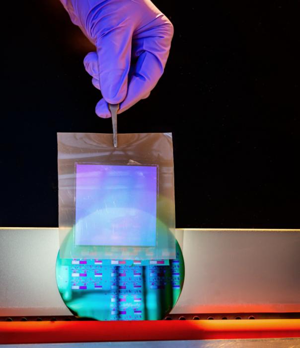
The Illinois method elegantly sidesteps the entire conundrum through a clever technique. Instead of growing the hot silicon onsite, the team cultivates it elsewhere, removes it as an exceptionally thin sheet, and applies it cold.
These sheets are nanomembranes of single-crystalline silicon, measuring 10 nanometers thick or less. (In comparison, a typical silicon wafer ranges from 500 to 700 micrometers, thousands of times thicker.) The films are detached from a donor wafer, lifted, and transfer-printed onto the receiving chip with a roll laminator, requiring no more than about 200 degrees for bonding. Due to their thinness, the membranes are flexible, capable of conforming over whatever surface lies beneath. “This conformability helps prevent interfacial defects like voids,” Cao points out, referring to the type of flaws that complicate efforts to bond two rigid wafers together.
Next came the issue of the transistors themselves. Constructing a conventional transistor involves “doping” silicon, introducing impurities to adjust its electrical properties, and doping is yet another process requiring high temperatures, often exceeding 600 degrees. Thus, the team employed a design known as a junctionless transistor, where the silicon is uniformly and heavily doped before stacking occurs. No high-temperature processing afterward, and no abrupt junctions need to form. Because the film is so thin, the gate can effectively switch the channel on and off. Utilizing this technique, they created three stacked layers, each bearing 625 transistors, and interconnected them into functioning logic gates and memory cells. Yields varied from 96 to 100 percent across about 3,750 devices, and the transistors delivered currents exceeding 650 microamps per micrometer, comfortably within the range of conventionally produced silicon using heat, and significantly better than alternative material competitors.
Such results, originating from an academic cleanroom rather than a multi-million dollar manufacturing facility, are what typically make the chip industry take notice.
There are, of course, caveats. The variability between devices is still greater than what a commercial foundry would accept, an issue the team attributes to the limitations of their university facilities rather than the technique itself. Furthermore, the gate insulation is thicker than that of the most advanced commercial chips, requiring the transistors to operate at slightly higher voltages. These are likely fixable issues, but they remain challenges nonetheless.
What a chip foundry would be eager to learn
What makes this result compelling beyond the lab is the timing. Vertical