Scientists have made remarkable progress in atomic manipulation, achieving unparalleled control over atomic placements on the mesoscopic scale, which serves as a link between singular atoms and bulk materials. By integrating 40,000 user-specified defects into a single crystal lattice, researchers have showcased the ability to accurately design materials with customized characteristics by meticulously modifying the atomic configurations within their frameworks.
Techniques for atomic manipulation have been fundamental to scientific progress for many years. The capability to relocate and arrange individual atoms through microscopy techniques has enhanced our comprehension of chemistry and material science. A significant achievement in this domain took place in 1990 when two IBM scientists utilized a scanning tunneling microscope to shift xenon atoms on a nickel surface, forming the logo of the IBM company, highlighting the possibilities of atomic-scale manipulation.
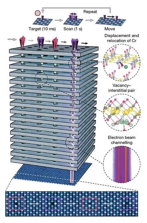
Expanding upon this critical research, a joint group from the US and Europe has elevated the idea to new heights. Using a specially designed scanning transmission electron microscope, the researchers incorporated defects into the chromium sulfur bromide (CrSBr) lattice. This semiconductor was selected as the model system due to its exceptional attributes, enabling the team to systematically relocate chromium atoms through an automated mechanism. This initiative has led to what they refer to as ‘a novel type of engineered artificial matter’ that remains stable at room temperature outside the microscope environment.
The accuracy of the method is remarkable; the defects were implanted within just minutes over a nanoscale area measuring 150nm by 100nm with a depth of 13nm. The researchers are hopeful that this approach can be generalized and scaled up to impact macroscopic materials, thereby paving the way for programmable matter where material functions are carefully engineered from the atomic level upwards.